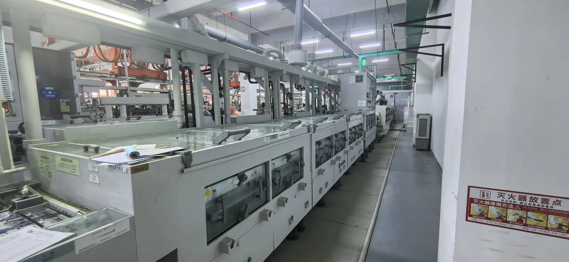

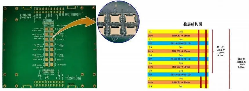
77 GHz radar high-frequency board
- Layers
- 18
- Materials
- TSM-DS3 + FR28 prepreg + S1000-2M, hybrid lamination
- Finish
- Immersion gold (ENIG)
- Special process
- Pure PTFE blind/buried-via impedance board, 5 back-drill groups
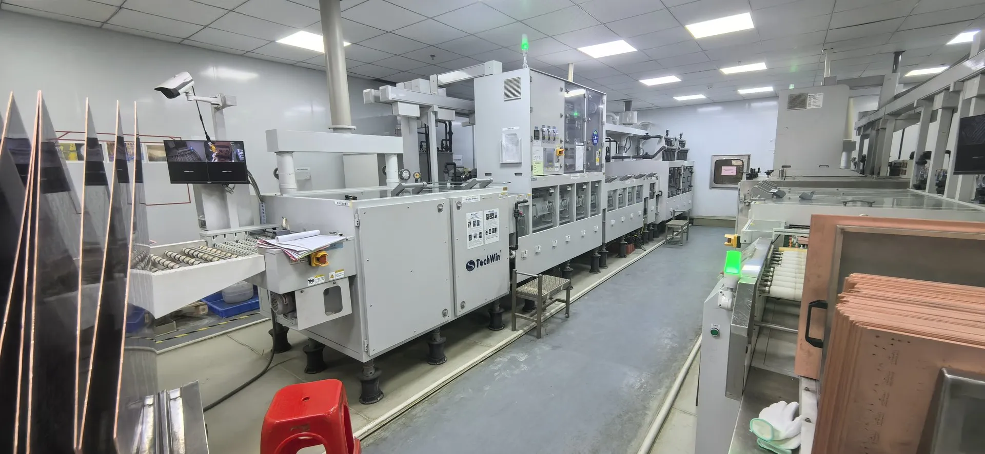
Circuit boards for RF and microwave designs where dielectric properties, loss and stability matter.
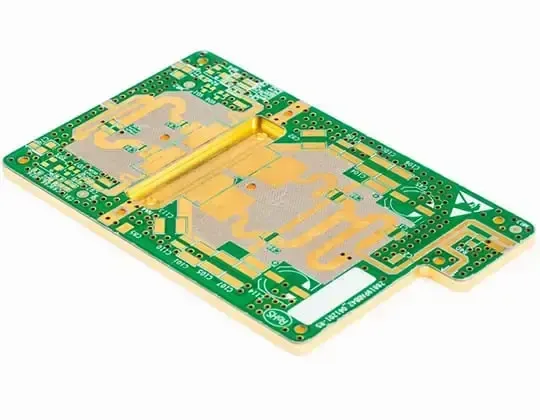
High-frequency boards rely on laminates such as Rogers, Isola and PTFE-based materials. We review your frequency, loss and stability targets, compare material options and confirm availability before quotation. Supplier datasheet values are material data, not fabrication guarantees.
| Positioning | Rogers / Isola / PTFE | |
|---|---|---|
| Standard / prototype | Advanced / mass production | |
| High-Frequency PCB | 24L | 20L |
Source: ShinePCB capability workbook, navigation overview. Values are confirmed against your files and the assigned facility during engineering review; certificates are available on request.
| Parameter | Prototype | Mass production |
|---|---|---|
| Material system | PTFE, hydrocarbon resin, other materials | PTFE + ceramic, PTFE + glass fiber + ceramic, PTFE + glass fiber |
| Layer count (max) | 24L | 20L |
| Panel size (max) | 850 × 700 mm | 720 × 650 mm |
| Profile tolerance | ±0.05 mm | ±0.10 mm |
| Slot tolerance | Normal slot ±0.08 mm, routed slot ±0.10 mm | Normal slot ±0.10 mm, routed slot ±0.13 mm |
| Layer registration | 2 mil | 3 mil |
| Hybrid lamination | PTFE + glass ceramic + FR-4 | PTFE + glass ceramic + FR-4 |
| Min hole size | 0.075 mm | 0.10 mm |
| Min hole spacing | 0.20 mm | 0.25 mm |
| Hole diameter tolerance | ±0.05 mm | ±0.075 mm |
| Max aspect ratio | 16:1 | 12:1 |
| Hole copper uniformity | COV ≤ 5% | COV ≤ 7% |
| Resin-filled via aspect ratio | 12:1 | 12:1 |
| Resin-filled via type | Through hole / blind via | Through hole / blind via |
| Trace width tolerance | ±0.6 mil | ±1 mil |
| Impedance tolerance | ±5% | ±8% |
| Warpage | 0.50% | 0.75% |
| Special processes | POFV (VIPPO), sequential lamination, local lamination, long/short gold finger, counterbore, back drill, side metallization, N+N structure, edge plating, thick copper, HDI | Same processes as prototype |
| Approved material brands | Shengyi, ITEQ, Taiwan Union, Panasonic (M4/M6/M7/M8), Rogers, Taconic, Wangling, Ventec, Isola | Same brands as prototype |
Source: ShinePCB capability workbook (high-frequency & high-speed sheet has no year column). Prototype and mass-production values are listed separately and are not interchangeable. Every value is confirmed against your files, the selected material and the assigned facility during engineering review.
| Material | Series | Tg | Dk | Df | Typical use |
|---|---|---|---|---|---|
| Rogers RO3003 | RO3000 | — | 3.00 @ 10 GHz | 0.0013 | Microwave and RF |
| Rogers RO3006 | RO3000 | — | 6.15 @ 10 GHz | — | Microwave and RF |
| Rogers RO3010 | RO3000 | — | 10.2 @ 10 GHz | — | Microwave and RF |
| Rogers RO3035 | RO3000 | — | 3.50 @ 10 GHz | 0.0017 | Microwave and RF |
| Rogers RO4003C | RO4000 | >280 °C | 3.38 (process Dk) @ 10 GHz | 0.0027 | RF and microwave; hybrid boards |
| Rogers RO4350B | RO4000 | >280 °C | 3.48 (process Dk) @ 10 GHz | 0.0037 | RF and microwave; hybrid boards |
| Rogers RO4360G2 | RO4000 | — | — | — | RF and microwave; hybrid boards |
| Rogers RO4835 | RO4000 | — | — | — | RF and microwave; hybrid boards |
| Rogers RO4450 | Bonding material | — | — | — | RF hybrid lamination bonding |
| Arlon CLTE | Ceramic-filled PTFE | — | — | — | RF and microwave |
| Taconic RF-35 | Ceramic-filled PTFE | — | — | — | RF and microwave |
| Shengyi SCGA-500 GF220 | PTFE RF laminate | — | 2.2 | 0.0009 | RF and microwave |
| Shengyi SCGA-500 GF255 | PTFE RF laminate | — | 2.55 | 0.0014 | RF and microwave |
| Shengyi SG7350D / SG7350D2 | RF and microwave | — | 3.55 | 0.0020–0.0022 | RF and microwave |
| Shengyi mmWave77 | Millimeter wave | — | 3.0 | 0.001 | Automotive radar and millimeter wave |
| Shengyi LNB33C series | RF and microwave | — | 3.30–3.50 | 0.003–0.0035 | RF and microwave |
Source: ShinePCB capability workbook, material sheet. Dk, Df and Tg are typical supplier datasheet values (test frequency shown where the source lists it). They describe the laminate, not the finished board. Grades are available on request and confirmed with availability during engineering review. "—" means no value is listed in the source.
Board constructions from the ShinePCB company presentation — not customer references.
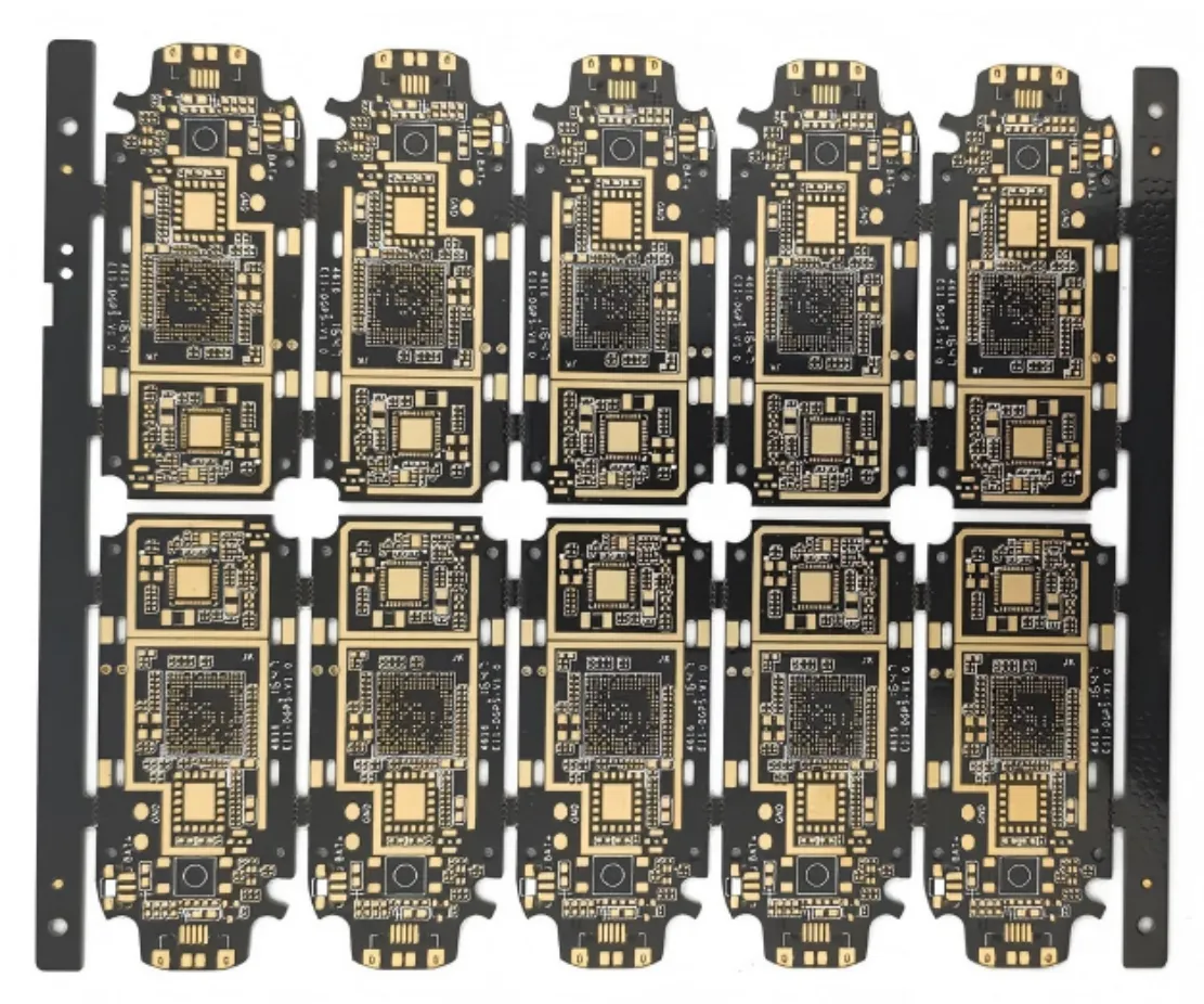
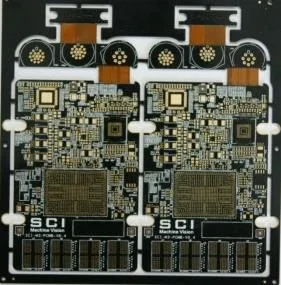
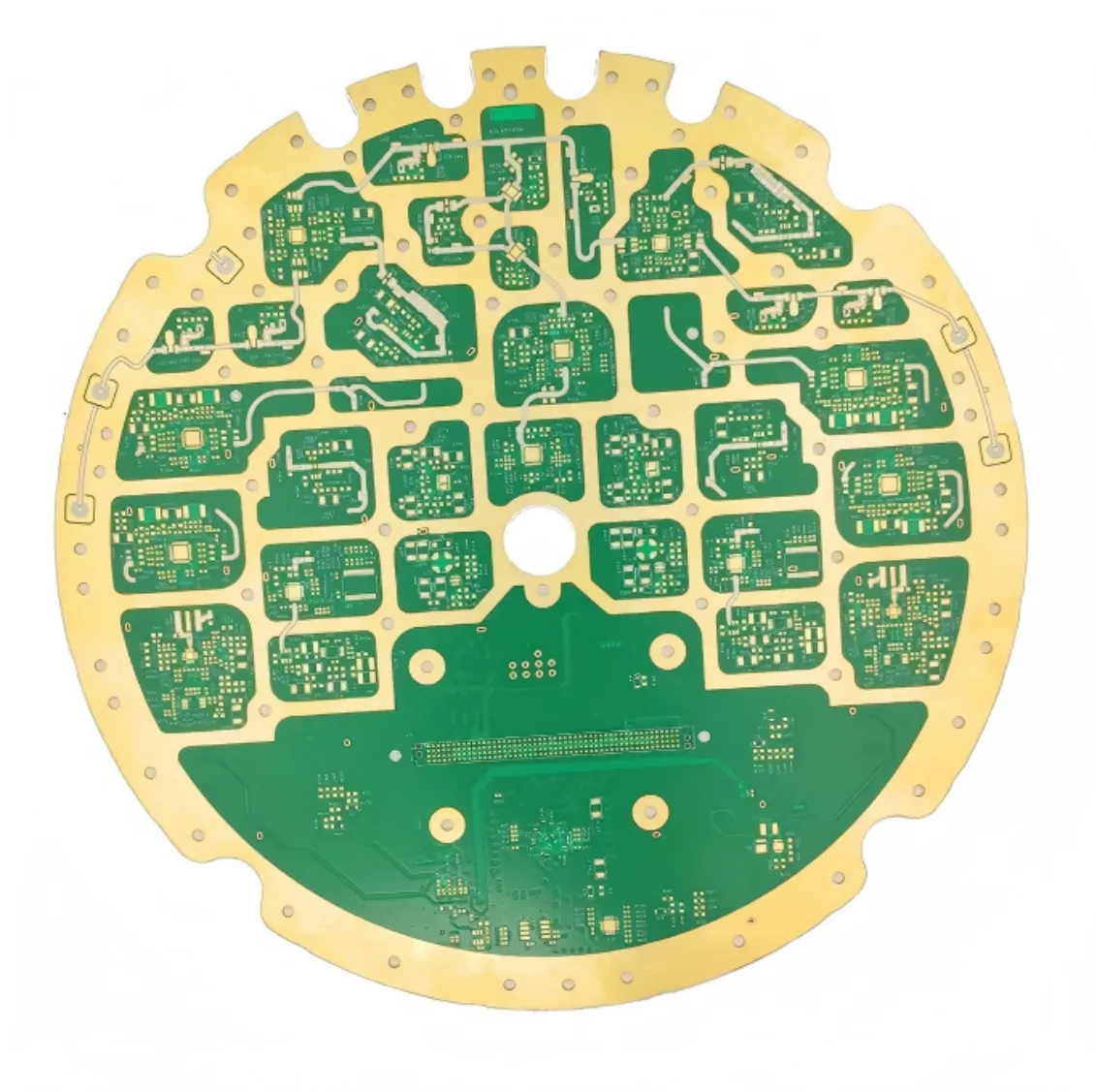
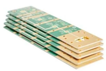
Builds from the ShinePCB company presentation. They illustrate process scope and are not customer references.
Every order follows the same controlled sequence. Prototype and production requirements are reviewed separately.
Gerber or ODB++, drill data, drawing and quantities are checked for completeness.
Open points on manufacturability, materials or special processes are sent before quotation.
Construction, laminate and finish are confirmed with you and written into the order.
The order is released to the facility whose process and qualification fit the requirements.
Inspection and electrical test follow the methods agreed for your order.
Boards are packed and shipped under the confirmed delivery terms.
Start with the details you have — engineering will request anything else needed for the review.
Customer Gerber, BOM and design data are managed under an ISO/IEC 27001 information security system and shared only within your project.
It depends on frequency, loss budget, thermal needs and cost. Share your targets and we will review suitable options.
Hybrid stack-ups are reviewed per project for compatibility and processing.